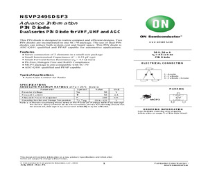
.com 3 NSVP249SDSF3 PACKAGE DIMENSIONS unit : mm SC-70 / MCP3 CASE 419AJ ISSUE O to *1 : Lot indicaon RECOMMENDED SOLDERING FOOTPRINT 2.1 1.0 0.7 1 : Anode 2 : Cathode 3 : Cathode / Anode 0.65 0.65 www.onsemi.com 4 NSVP249SDSF3 ORDERING INFORMATION Device NSVP249SDSF3T1G Marking Package Shipping GV SC-70 / MCP3 Pb-Free / Halogen Free) 3,000 / Tape & Reel For information on tape and reel specifications, including part orientation and tape sizes, please refer to our Tape and Reel Packaging Specifications Brochure, BRD8011/D. http://www.onsemi.com/pub_link/Collateral/BRD8011-D.PDF ON Semiconductor and the ON Semiconductor logo are trademarks of Semiconductor Components Industries, LLC dba ON Semiconductor or its subsidiaries in the United States and/or other countries. ON Semiconductor owns the rights to a number of patents, trademarks, copyrights, trade secrets, and other intellectual property. A listing of ON Semiconductor's product/patent coverage may be accessed at www.onsemi.com/site/pdf/Patent
 5 Pages, 407 KB, Original
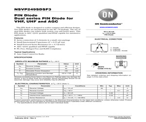
. IR -VR Figure 4. rs - f www.onsemi.com 2 5 7 1000 2 NSVP249SDSF3 1k 7 5 TA = 25C f = 100 MHz 3 Resistance, rs - W 2 100 7 5 3 2 10 7 5 3 2 1.0 0.01 2 3 5 7 0.1 2 3 5 7 1.0 2 3 5 7 10 Forward Reverse, IF - mA Figure 5. rs - IF ORDERING INFORMATION Device NSVP249SDSF3T1G Marking Package Shipping GV SC-70 / MCP3 (Pb-Free / Halogen Free) 3,000 / Tape & Reel For information on tape and reel specifications, including part orientation and tape sizes, please refer to our Tape and Reel Packaging Specifications Brochure, BRD8011/D. www.onsemi.com 3 MECHANICAL CASE OUTLINE PACKAGE DIMENSIONS SC-70 / MCP3 CASE 419AJ ISSUE O DOCUMENT NUMBER: 98AON65442E DATE 30 NOV 2011 Electronic versions are uncontrolled except when accessed directly from the Document Repository. Printed STATUS: ON SEMICONDUCTOR STANDARD versions are uncontrolled except when stamped "CONTROLLED COPY" in red. NEW STANDARD: (c) Semiconductor Components Industries, LLC, 2002 Case Outline Number: http://onsemi.com October, DESCRIPTION: 2002 -
 6 Pages, 145 KB, Original


